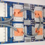

For decades, the hardest part of building a processor has not been the factory. It has been the months of painstaking work by human engineers who write, rewrite and verify the code that describes every adder, multiplier and data path on the die. On 18 November 2026, OpenAI published a detailed account claiming that its models are now doing a measurable share of that work, and doing it well enough that AMD has already put some of the results into a chip sent for manufacturing. In this Technology analysis I look at what was actually announced, what the headline 14% figure means, and where the caveats lie.
What OpenAI Announced on 18 November
The announcement came as a technical post on OpenAI’s site, “Advancing chip design with OpenAI models”, dated 18 November 2026. It makes three distinct claims. First, that model-proposed changes measurably improved Jalapeño, OpenAI’s first custom inference chip, and that those changes were “silicon proven” when the chip came back from the fab. Second, that a collaboration with AMD produced “up to 14% improvement relative to heavily optimized baselines on the flagship GPU IP,” plus single-digit gains on key blocks of AMD’s next flagship CPU. Third, that successive generations of OpenAI models are getting steadily better at a reproducible chip-design benchmark built on open-source RISC-V processor cores.
The story was quickly picked up by the specialist press. The Next Web reported it the same day, noting that some of the model’s circuit changes are already in a chip AMD has sent for manufacturing. DatacenterDynamics and Tom’s Hardware followed with their own breakdowns of the figures. It is worth stressing from the outset that all of the numbers originate from OpenAI’s post; AMD’s verification of the CPU gains is reported by OpenAI rather than in a separate AMD statement.
Inside the 14%: Power, Performance and Area
To understand the claim you need one acronym: PPA, for power, performance and area. These are the three quantities every chip designer trades against each other. A circuit can be made faster by adding hardware, but that costs silicon area and energy; it can be made smaller, but often at the cost of speed. An improvement in PPA means getting a better combination of the three for the same function. On a flagship GPU, where every square millimetre of a leading-edge wafer is expensive and every watt matters inside a data centre, gains of a few percent are normally the product of long, incremental engineering.
According to OpenAI, its model found its improvements by rewriting the chip’s SystemVerilog RTL, the register-transfer-level code that describes how each circuit behaves before it is turned into physical transistors. The company says the model can rewrite circuits “that perform calculations, control operations, or move data,” and that it reasoned about RTL “at the level of an expert microarchitect.” Crucially, it used Synopsys tools to verify that each rewrite preserved the original block’s behaviour and to measure the resulting trade-offs.
OpenAI characterises the result as “roughly a year of progress achieved in less than 5 months.” AMD, it says, has already included some of the changes in a recent design sent for manufacturing and added others to its production design files for future versions. On the CPU side, AMD verified single-digit percentage gains in PPA across key blocks of its upcoming next-generation flagship processor using designs written by the model. Neither OpenAI nor the coverage names the specific AMD products, and the post does not break the 14% down into separate power, speed and area components.

Jalapeño: The In-House Proof Point
The AMD numbers are the headline, but the Jalapeño results are arguably the stronger evidence, because they have already passed through real silicon. OpenAI says it began using its models to help design the chip in early 2025, and that even that early model made “nontrivial” PPA improvements. The Next Web adds that Jalapeño went from design to manufacturing in nine months.
The details are specific. In the matrix unit, one multiplier redesign used about 15% less cell area in synthesis while cutting latency from two clock cycles to one, a rare case of a change that is both smaller and faster. A separate adder redesign reduced cell area by about 15% while keeping its two-cycle latency. In the vector unit, which handles parallel computing tasks, savings came from floating-point adders and multipliers, conversion functions, reduction logic and the special-function unit. Across the wider effort, OpenAI estimates that model-proposed changes reduced standard-cell area by about 13% in the vector unit and 10% in the matrix unit.
For anyone following the economics of semiconductors, this is the interesting part. Area translates directly into cost: smaller blocks mean more dies per wafer or more room for additional compute. If AI-assisted design can reliably shave double-digit percentages off arithmetic units that engineers already considered mature, the payoff compounds across every chip produced.
A Benchmark Built on Open-Source RISC-V Cores
Production results are hard to reproduce outside a company, so OpenAI also described a more controlled test. It took two open-source 32-bit RISC-V cores: PicoRV32, a compact core designed for FPGAs, and Ibex, the embedded processor used in the OpenTitan security chip. Models were given the original hardware description and asked to increase throughput, the number of instructions the core can execute per second.
The scoring rules are strict. Designs were checked in simulation and scored zero if they failed a check or used more than 16 times the original core’s area. For passing designs, OpenAI measured instructions per clock cycle on workloads hidden from the models and multiplied the result by the maximum clock frequency estimated with the open-source Yosys synthesis tool. The best throughput observed under the same constraints was assigned a score of 1.0. According to DatacenterDynamics, five models were tested: GPT-5.5, GPT-5.5 Sol, GPT-6.1 Sol, GPT-6 Astra and GPT-6.2 Astra.
At a comparable budget of about 112,000 tokens per run, GPT-6.2 Astra had the highest average score on both cores; on PicoRV32 its score was about twice that of GPT-6 Astra. In a second task, the models designed a core from written requirements instead of improving existing code, and all five scored higher. OpenAI itself flags why: starting from a specification lets the models omit features such as performance counters and extra instructions that may not help on the test workloads. The full evaluation included 9,881 scored runs. The company also concedes that requiring those features, setting tighter area limits and checking timing after physical synthesis would make the test more representative of production design.
GPT-Synopsys and the Future of the Toolchain
The last section of OpenAI’s post points to what comes next: a partnership with Synopsys to train GPT-Synopsys, a model meant to use Synopsys’ electronic design automation (EDA) tools “the way expert chip designers do.” That partnership was first announced on 30 September 2026. In Synopsys’ press release, the companies described a multi-year agreement under which OpenAI licenses Synopsys EDA tools, the two collaborate on R&D and go-to-market, and revenue is shared. Engineers would delegate objectives from PPA optimisation to timing and verification closure, with agents running tools, interpreting results and iterating “toward verified outcomes for engineer review.” Reuters reported at the time that the model would be trained for tasks spanning from code-like circuit descriptions to laying out billions of transistors.
This framing matters. The industry already relies on a small number of EDA vendors whose tools act as the ground truth for whether a design works. OpenAI is not proposing to replace that layer; it is proposing to put a reasoning model on top of it, with the established verification tools as referee. That is the same pattern visible in the AMD work, where Synopsys tools checked every rewrite. OpenAI has not said when GPT-Synopsys will be available.

Caveats, Trust and What to Watch
Three cautions are in order. The first is provenance: the AMD figures come from OpenAI’s own post, and the coverage so far relays them rather than offering independent measurements. The second is scope: “up to 14%” describes the best result on specific blocks against a heavily optimised baseline, not a 14% better GPU overall. The third is trust. As The Next Web notes, OpenAI’s own chip chief, Richard Ho, said last month that he still does not fully trust AI design changes, which is why every one is checked.
That last point is not a weakness of the approach; it is the approach. The most credible version of chip design with AI is not an autonomous model shipping silicon, but a model proposing rewrites at machine speed while formal verification and human review decide what survives. If that loop holds up, the bottleneck in building new accelerators shifts from the number of senior microarchitects a company can hire to the quality of its verification infrastructure.
What to watch next: whether AMD discusses these gains when its next flagship GPU and CPU are formally unveiled, whether GPT-Synopsys reaches customers and on what terms, and whether rival chip designers report similar results with their own tools. There is also a striking feedback loop here. AI models are now helping to design the chips that will train and run the next generation of AI models. If the gains OpenAI describes are repeatable, that loop could tighten faster than the industry’s traditional design cycles have ever allowed.